Understanding IPC Standards for PCB Design
IPC Guidelines Built Into Neurocad
IPC standards provide a common engineering framework for designing, manufacturing, assembling, and inspecting electronic products. They help electronics engineers make consistent decisions about PCB footprints, land patterns, spacing, solder paste, component assembly, manufacturing data, and workmanship requirements.
Neurocad applies applicable IPC guidance during engineering asset creation so important manufacturing and assembly considerations can become part of the design data earlier in the workflow. The standards below are currently incorporated into Neurocad. Additional standards will be added over time.
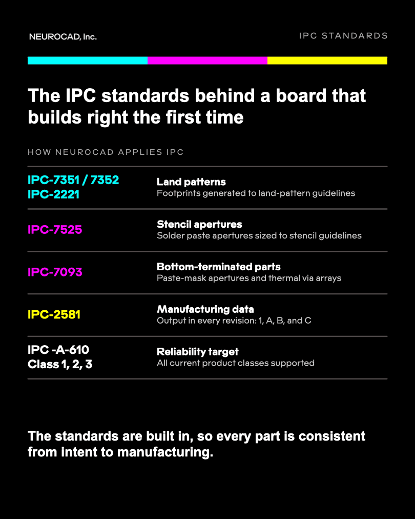
IPC-7351 and IPC-7352: PCB Land Patterns and Footprints
What it covers:
IPC-7351 and IPC-7352 provide guidance for creating PCB land patterns used to mount and solder electronic components. The guidance addresses pad geometry, component dimensions and tolerances, solder-joint requirements, solder-mask clearances, paste apertures, courtyards, spacing, orientation, and related ECAD library data. IPC-7351 focuses on surface-mount design, while IPC-7352 provides current generic land-pattern guidance.
Why it matters:
The PCB footprint connects the component specification to the physical board. Accurate, consistent land patterns improve solder-joint formation, component placement, inspection, testing, rework, and CAD library consistency.
Engineering takeaway:
Use standardized land-pattern geometry as the baseline, then account for the component manufacturer’s dimensions, fabrication capabilities, assembly process, and product requirements.
IPC-2221: Printed Board Design
What it covers:
IPC-2221 is the generic foundation for printed board design. It establishes design principles for conductors, electrical spacing, materials, dielectric properties, vias, component mounting, thermal considerations, electrical testing, and other board-level requirements. More specialized IPC-2220-series standards provide additional guidance for technologies such as rigid, flex, and HDI printed boards.
Why it matters:
PCB geometry affects electrical performance, manufacturability, insulation, thermal behavior, and long-term reliability. IPC-2221 gives engineers a common starting point for translating electrical and mechanical requirements into physical PCB design rules.
Engineering takeaway:
Apply IPC-2221 with the actual voltage, environment, stackup, impedance requirements, fabrication capabilities, and technology-specific standards for the product.
IPC-7525: Stencil and Solder-Paste Design
What it covers:
IPC-7525 provides guidance for stencil design and fabrication for solder-paste printing and surface-mount adhesive. It addresses stencil apertures, stencil thickness, aperture geometry, area and aspect ratios, and other factors that affect paste transfer.
Why it matters:
The copper pad defines the connection area. The stencil controls how much solder paste reaches that area. Aperture geometry and stencil thickness directly affect paste volume, transfer efficiency, bridging, opens, tombstoning, voiding, component movement, and assembly yield.
Engineering takeaway:
Design the copper land pattern and paste pattern together. Fine-pitch components, exposed thermal pads, and bottom-termination packages often require specific aperture strategies to achieve consistent solder joints.
IPC-7093: Bottom-Termination Components
What it covers:
IPC-7093 provides design and assembly guidance for bottom-termination components, including QFN, DFN, SON, LGA, MLP, and MLF packages. It addresses land patterns, exposed thermal pads, thermal vias, solder paste, assembly, inspection, repair, quality, and reliability.
Why it matters:
BTC solder joints sit underneath the component, where direct visual inspection is limited. Reliable assembly depends on the interaction among pad geometry, thermal-pad design, via strategy, solder volume, stencil apertures, reflow, inspection, and rework.
Engineering takeaway:
Treat the footprint, thermal system, and solder-paste strategy as one assembly problem. Validate the final implementation against the specific component, PCB fabrication process, and assembly process.
IPC-2581: Digital PCB Manufacturing Data
What it covers:
IPC-2581 defines an XML-based format for exchanging structured PCB and PCB-assembly manufacturing data. A package can carry board geometry, copper, nets, pads, vias, drill data, stackup, materials, component placement, BOM information, assembly information, manufacturing details, and traceability data in a machine-readable product definition.
Why it matters:
PCB manufacturing releases often distribute design intent across multiple files. A structured digital product definition gives fabrication, assembly, inspection, and manufacturing systems richer engineering context and reduces opportunities for manual interpretation, missing information, and revision mismatches.
Engineering takeaway:
Use IPC-2581 to preserve structured design and manufacturing information across the ECAD-to-manufacturing handoff, then validate the manufacturing package against supplier DFM, DFA, test, process, and product requirements.
IPC-A-610: Electronic Assembly Acceptability
What it covers:
IPC-A-610 establishes visual acceptance criteria for completed electronic assemblies. It addresses solder connections, component placement and installation, terminations, cleanliness, markings, coatings, physical damage, and other visible workmanship conditions. IPC-A-610J is the current revision published by IPC.
Why it matters:
A shared acceptance standard gives engineering, manufacturing, inspection, quality, suppliers, and customers consistent criteria for evaluating completed electronic assemblies.
Engineering takeaway:
Specify the applicable IPC-A-610 revision and product class in the engineering and manufacturing requirements. The selected class determines which acceptance criteria apply to the product.
IPC Classes 1, 2, and 3: Product Performance Requirements
IPC product classes define different performance and reliability expectations for electronic products. The appropriate class should be established from the product’s intended use, operating environment, reliability requirements, and contractual requirements.
Class 1: General Electronic Products
Applies when functional operation of the completed assembly is the primary requirement.
Class 2: Dedicated Service Electronic Products
Applies when continued performance and extended service life are required and uninterrupted operation is desirable.
Class 3: High Performance / Harsh Environment Electronic Products
Applies when continued or on-demand performance is critical, equipment downtime carries significant consequences, or the product operates in demanding environments.
The selected class can influence workmanship acceptance, manufacturing controls, inspection, documentation, traceability, supplier requirements, cost, and production planning. Class should therefore be established during product definition and carried through design, procurement, manufacturing, and inspection requirements.
Why IPC Guidelines Matter in PCB Design
PCB design decisions move downstream. A land pattern affects soldering. Solder-paste geometry affects assembly. Board geometry affects fabrication and electrical performance. Manufacturing data affects how design intent reaches the factory. Acceptance criteria determine how the finished assembly is evaluated.
Using recognized IPC guidance gives electrical engineers, PCB designers, manufacturers, and quality teams a shared engineering language across those decisions.
Neurocad brings applicable IPC guidance into the engineering workflow so standards-aware decisions can be applied when design assets are created, rather than treated as disconnected information later in the product-development process.
Show us what you're stuck on.
We'll build it in a live demo.
Last updated September 30, 2026